| Vocademy |
Part 3: How Microprocessors Work
The long-obsolete 6502 microprocessor is popular in Computer Science curriculums as a teaching tool. This is because of its simplicity. The 6502 was the primary inspiration for modern RISC (Reduced Instruction Set Computer) processors and will be used here to show how microprocessors work
Understanding a basic microprocessor
The basic operations of a microprocessor are to:
-
Retrieve a byte of data from memory.
-
Optionally manipulate the byte of data.
-
Put a byte of data into memory.
There's really not much more to it than that.
The microprocessor is connected to memory through an array of wires that select and manipulate memory.
The address bus
The address bus is a collection of pins or wires that connect the microprocessor to the memory subsystem and allow the CPU to select a single byte of memory by specifying its address. Consider the Jacquard loom and its punched cards. If you number the cards in sequence, a memory address is like the number of a particular card. Think of it as if the loom were able to request a certain card by its number. The address buss allows the CPU to select a certain byte of memory by its address. The 8080 and the 6502 had 16-bit address busses (16 pins or wires) and could therefore select any of 65,636 bytes of memory.
Extra study material:
Note: the following material with a gray background is of little use to most computer technicians. However, if you are interested in robotics, embedded systems, microcontrollers, etc., the following will give you insight into how the circuits are wired. This is not required reading, and you will not be tested on the material.
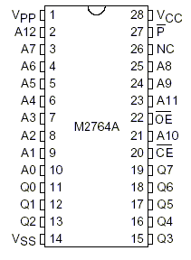
To understand the address bus let's examine a single memory chip. A good chip for this example would be a 2700 series EPROM chip. The 2764 holds 8,192 bytes (8 kiB) of memory.
 |
| Pinout of the 2764 EPROM chip. |
There are 13 pins on the 2764 that are used to specify exactly which of these bytes of memory to access. These pins are numbered A0 � A12. To access byte number 128, the binary number to put on these pins is 00010000000. To access byte 129, that would be 00010000001. Byte 130 would be 00010000010, and so on.
The data bus
The data bus consists of a group of wires that move data in and out of the microprocessor. Like the address bus, the data bus is connected to the memory and input/output subsystem. Computers and operating systems are classified by the data bus's width (number of wires). Early computers had eight-bit-wide data busses and could manipulate one byte at a time. Most computers now have 64-bit-wide data busses and can manipulate eight bytes at a time.
ROM
ROM is Read-Only Memory. It is memory that cannot be changed. ROM is often called "firmware" because it is hardware that contains permanent software--a hybrid of hardware and software. Computers use programming in ROM to start up, when RAM is empty (see below). ROM chips may be manufactured with data already stored in them. Programmable ROM (PROM) can be programmed once but the data cannot be changed. Erasable PROM chips (EPROM) are erased by exposure to ultraviolet light and can be reprogrammed. Electrically erasable EPROM chips (EEPROM) are erased by an erase function built into the chip. All of the above chips must be erased all at once and so are not suitable as a main memory where data is often erased a byte at at time. Therefore, they are all used like ROM chips. Modern computers us what is called non-volitile RAM (NVRAM) in place of ROM. NVRAM can be erased in small blocks and so can be used more like RAM. Solid State Drives use NVRAM.
Connecting to a 6502
ROM
The following is an example of how a microprocessor connects to memory and I/O devices. A 6502 microprocessor has 16 address pins and 8 data pins. If a single 2764 were the only memory available, there would be a fairly straightforward connection between the microprocessor and the memory chip. Essentially, the first 13 address pins of the 6502 would connect to the 13 address pins of the 2764. All 8 data pins of the 6502 would connect to the 8 data pins of the 2764. When the 6502 needs to access a byte of data, it puts the address of that byte on the address pins and accesses the data via the data pins.
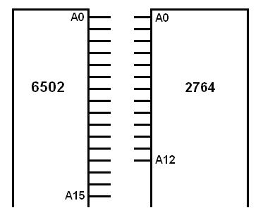
What happens if you have two 2764s to yield 16k of memory? How would you connect the two memory chips to the microprocessor? As you can see in the illustration below, the 6502 has three more address pins than the 2764.
 |
| The 6502 has three more address pins than the 2764. |
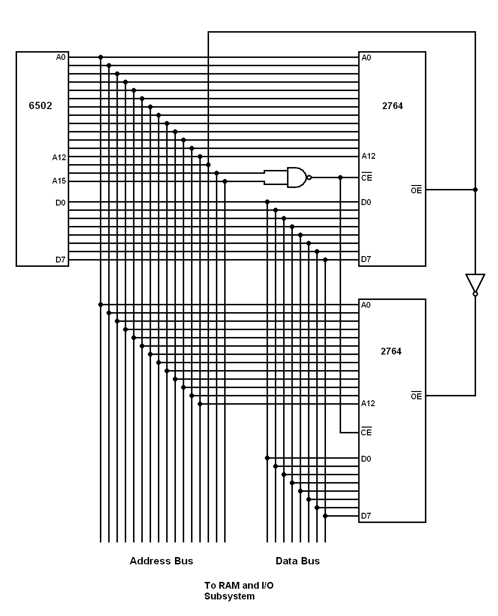
You can use the 14th pin of the 6502 address bus to select between two 2764 memory chips. The first 13 pins will connect in parallel to both 2764s. These pins can select any one of the 8,192 bytes of memory available in either 2764. The 14th pin selects which of the two 2764s to access. The 14th pin will connect directly to the Output Enable pin of one 2764 and through an inverter to the Output Enable pin of the other 2764.
The following diagram shows a more-real-world example of connecting a 6502 to two 2764s. A NAND gate is connected to the 15th and 16th pins of the 6402 with the output going to the Chip Enable pins of both 2764s. The only time both the 15th and 16th address pins of the 6502 are high is when it is accessing the highest 16k of its memory space. This puts the ROM chips at the high end of the memory space leaving the low end available for RAM.

| Two 2764s connected to a 6502 to be the last 16 kiB of memory. A 2764 is fully enabled when both the /CE and /OE pins have a logical 0. When both A14 and A15 are logical 1, both /CE pins are enabled through the NAND gate. Then line A13 chooses between the two chips. If A13 is 0, the top 2764 is enabled, and if it is 1, the bottom 2764 is enabled. If the address bus has any number lower than 0010000000000000, neither chip is enabled and the processor can communicate with the RAM subsystem or the I/O subsystem. |
The address and data bus connect to the RAM and I/O subsystem. Other gates there determine which RAM chips or I/O devices to connect to the data bus depending on what address is specified on the address bus.
RAM
RAM is Random Access Memory. Random access means that the computer can jump to any location in memory without passing by other locations. This is unlike such systems as magnetic tape memory that was once common with computers. ROM is also accessed randomly so the name RAM may be a bit misleading. The main difference between ROM and RAM is that when the computer starts the RAM is empty. Information is loaded into RAM during the startup process and while the computer is being used. RAM is also typically volitile (dynamic RAM). This means that the chips lose their information shortly after it is stored (it sort of evaporates). The reason is that the volitile chips are less expensive and store more information than equivalent non-volitile memory (such as non-volitile RAM). Dynamic RAM chips lose information after about 100 milliseconds. The RAM subsystem includes circuitry that "refreshes" the RAM about every 50 milliseconds (typically 64ms). The microprocessor connects to the RAM subsystem and is not involved in the refresh process.
Another significant difference is that early RAM chips had only a single data wire. The address bus specified an address, and a single bit was returned. A bank of 8 RAM chips was required to manage 8-bit bytes. Yet another major difference was that RAM chips multiplexed the address bus in order to save pins on the package.
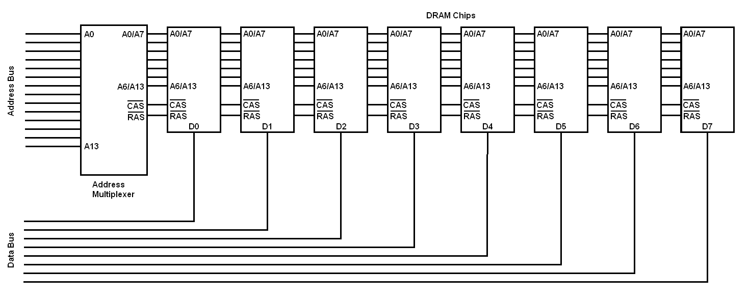
The following diagram shows a bank of eight 16 kib (16 kilobit) RAM chips and the address multiplexer required to manage the address bus. A 16 kib RAM chip requires a 14-bit address bus. This is sent to the address multiplexer, which sends 7 bits at a time to all the RAM chip's address wires. The first half of the address is put on the chip address bus then the CAS wire (Column Address Select) is toggled from the logical high state to the logical low state to load the address. Next, the second half of the address is put on the chip address bus then the RAS wire (Row Address Select) is toggled low to load that part of the address (the CAS and RAS lines control D-type latches in the chip). Then the Output Enable wire (not shown) is toggled low to connect the chips to the data bus. 8 RAM chips working together provide an entire byte to the data bus. Using this method, eight 16 kib chips (16 kilobits) provide 16 kiB of RAM (16 kilobytes).
 |
| A bank of eight 16k DRAM chips with their address multiplexer |
Modern computers have sophisticated memory controllers that handle RAM, ROM, and I/O devices. The microprocessor has to go through the memory controller to access any type of memory or I/O devices. The above example is intended to give a simple overview of how memory and I/O devices are connected to the microprocessor. Some modern RAM chips tend to handle multiple bits at a time, so a 64-bit-wide memory bank can be made with eight 8-bit wide chips.
| Vocademy |
