| Vocademy |
Semiconductors
Metals conduct electricity because of
the free electrons floating like a gas in the crystal structure. Most
non-metals do not conduct electricity because they form atomic
structures that do not provide free electrons. Materials that have a
conductivity between that of a conductor and a nonconductor are called
semiconductors. Semiconductors tend to have three to five electrons in
the outermost electron shell (the valence shell, where all chemical and
electrical action takes place).
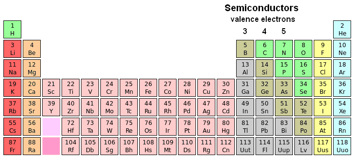
| Periodic table of the elements highlighting semiconductors |
When semiconductor materials are
mixed in certain ways, they can be used to control electrical current. Using photographic techniques, semiconductor
devices can be made small enough that millions of interconnected
devices can fit into a very small space. This has led to powerful
electronic equipment in very small packages. For example, the computing
power in a cell phone would have required a large air-conditioned room
only 40 years ago.
Semiconductor devices
Silicon is used for the basis of most
semiconductor devices. Germanium is occasionally used for semiconductor
devices. The properties of germanium devices differ from silicon
devices. However, the following discussion on semiconductor materials
applies to germanium as well as silicon.
A silicon atom has four electrons in its valence shell. When silicon forms a crystal, each of the four valence electrons will bond with the valence shell of an adjacent silicon atom. Once the crystal is formed, each silicon atom is surrounded by eight electrons. This forms what is called a covalent bond and is a very stable structure that leaves no free electrons to conduct electricity.
A silicon atom has four electrons in its valence shell. When silicon forms a crystal, each of the four valence electrons will bond with the valence shell of an adjacent silicon atom. Once the crystal is formed, each silicon atom is surrounded by eight electrons. This forms what is called a covalent bond and is a very stable structure that leaves no free electrons to conduct electricity.
| Intrinsic
silicon. Each silicon atom is surrounded by eight electrons, making the
structure electrically stable and a poor conductor. |
N-Type material
An arsenic atom has five electrons in
its valence shell. If a relatively few arsenic atoms (or another
element with five valence electrons) are introduced into a silicon
crystal, four of the electrons of each atom will bind with the valence
shells of adjacent silicon atoms. The arsenic will fit into the crystal
lattice. Each arsenic atom is now surrounded by eight bonded electrons
and the structure is stable. However, the crystal lattice is sort-of
like musical chairs. As a metaphor, there are only eight chairs
surrounding each atom (silicon or arsenic). There is no "chair" for the
fifth electron that belongs to the arsenic atom in the crystal lattice.
Since the fifth electron cannot bind with the crystal lattice, is
floats freely in the vicinity of its arsenic atom. The arsenic atoms
are said to donate an extra electron to the crystal lattice and are
called donor atoms. The extra electrons are called donor electrons. The
donor electrons act much like the electrons in metals, floating freely
like a gas molecule. Since the donor electrons carry a negative charge
this called N-type material. The N-type material is electrically
neutral. There is one proton for every electron in the material, so the
N-type material does not carry a negative charge. It just has an
abundance of free negative charge carriers—the donor electrons.
| N-Type Silicon Look carefully at the diagram above. A small number of arsenic atoms
(gray circles) are introduced into the crystal matrix. The arsenic
atoms leave extra electrons (black dots) that can move freely around
the matrix, making N-Type silicon a moderate conductor.
|
Phosphorus, antimony and bismuth also have five valence electrons and are used to make N-type material.
P-Type material
A gallium atom has three electrons in
its valence shell. If a relatively few gallium atoms (or another
element with three valence electrons) are introduced into a silicon
crystal, the three electrons will bind with the valence shells of
adjacent silicon atoms. However, since the gallium atom has only three
electrons in its valence shell, there will be only seven electrons
around the each gallium atom. A crystal structure is most stable when
each atom is surrounded by eight electrons. This shortage of an
electron around the gallium atom is called a "hole". Since silicon
doped with gallium has fewer electrons than intrinsic silicon—and
therefore has less negative charge carriers—it is called P-Type
silicon.
These holes in the crystal structure are very attractive to electrons and will tend to pull free electrons into the crystal and into the holes. These electrons will not bind into the crystal lattice because they need the attractive force of a proton to do so. Since every proton in the gallium atom is already bound to an electron, free electrons cannot bind into the crystal lattice. This leaves free electrons floating in the P-Type silicon, making it a moderate conductor.
These holes in the crystal structure are very attractive to electrons and will tend to pull free electrons into the crystal and into the holes. These electrons will not bind into the crystal lattice because they need the attractive force of a proton to do so. Since every proton in the gallium atom is already bound to an electron, free electrons cannot bind into the crystal lattice. This leaves free electrons floating in the P-Type silicon, making it a moderate conductor.
|
P-Type silicon.
Now look carefully at this diagram. A small number of gallium atoms (gray circles) are introduce into the crystal matrix. The gallium atoms cannot fill the spaces for eight electrons around the atoms, leaving a "hole" (missing gray dots). Free electrons introduced into the crystal are strongly attracted to the holes but can move about freely, making P-Type silicon a moderate conductor. |
Holes vs electrons
A strange thing appears to happen in P-Type semiconductor material. Just like N-type material the electrical current in P-type material consists of moving electrons. However, when analyzing P-type material it is difficult to follow the electrons. Instead, it appears that the holes move instead.To illustrate this let's play a little golf. While putting you notice the positions of the holes on the greens.
 |
| First day of golf. The hole is on the left side of the green. |
The next day you play another round and notice that all the holes have moved.
 |
| Second day of golf. The hole is now on the right side of the green. |
Between your rounds the greenskeeper cut new holes and used the material from the new holes to fill the old holes. You were fooled. The holes didn't move. It looks for all the world like the hole moved in one direction, but it was actually the grass and soil that moved in the opposite direction. When you get to the 19th hole what are you going to say to your buddies? In all honesty you would say, "They moved the holes since yesterday." Your buddies would know exactly what you mean and might explain that they do that almost every day. What would happen if you said, "They moved the soil since yesterday." Your buddies would have no idea what you were talking about. You and everyone else know fully well that it was the soil that was actually moved. However, the holes are what you see and moving holes has meaning where moving soil doesn't. You no more say the soil moved that you watch a sunrise and call it an Earth rotation. The holes moved and that is that.
Trying to understand current flow in P-type material by following the electrons doesn't work. It's like trying to follow the soil from hole to hole on the golf green. It's just something we don't wrap our minds around very well. In P-type material the holes are conspicuous, the electrons are not. Let's ignore the electrons, pretend they don't exist and just follow the holes.
In P-type material the holes are the charge carriers. They carry a positive charge and act opposite to the electrons in N-type material.
A P/N junction
For an electron to bind into a
crystal lattice it needs two attractive forces: a place to bind to in
the lattice and a nearby proton that is not associated with another
electron. If P-type silicon and N-type silicon are brought into
contact, the donor electrons in the N-type silicon will be strongly
attracted to the holes in the P-type silicon. These electrons will
travel into the P-type material on the other side of the junction. The
donor electrons cannot travel far from the N-type material because they
are also strongly attracted by their respective protons the arsenic
atoms. However, they can travel a short distance into the P-type
material. Once in the P-type material, these electrons can bind with
the holes in the crystal lattice there. Since these electrons have
found a place to bind to in the lattice and are still bound to protons
in the nearby arsenic atoms, they can from a bond in the crystal
lattice of the P-type material. This bond will be strong enough that
the electrons are no-longer free to move.
Once the electrons near the junction in the N-Type material have bound to holes near the junction in the P-Type material, there are no-longer any charge carriers in that region to allow the flow of electricity. This region is depleted of charge carriers and is called the depletion region. With no free charge carriers it is an insulator.
Once the electrons near the junction in the N-Type material have bound to holes near the junction in the P-Type material, there are no-longer any charge carriers in that region to allow the flow of electricity. This region is depleted of charge carriers and is called the depletion region. With no free charge carriers it is an insulator.
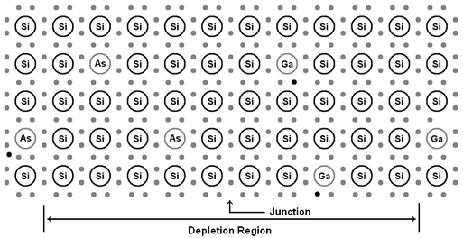
| Notice
that near the junction the extra electrons donated by the arsenic atoms
(black dots) have moved across the junction to the holes left by the
gallium atoms. The region where electrons have moved into holes is
called the depletion region. With no free charge carriers the depletion
region cannot carry electrical current and acts as an insulator. |
At this point the P-Type and N-Type material can be considered to be blocks of material that contain free charge carriers. The N-Type material has electrons that carry a negative charge and the P-Type material has holes that carry a positive charge. When N-Type material and P-type material are in contact with each other, the charge carriers disappear from the depletion region near the junction.
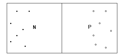
| Another View of a P-N Junction |
Electrons (dots) in the N-type silicon near the junction have migrated to fill the holes (circles) in the P-type silicon near the junction. Charge carriers no longer exist near the junction. The depletion region is the region devoid of charge carriers and acts as an insulator.
Forward and Reverse Biasing
If you place a voltage across silicon with a P-N junction, with the N side more positive than the P side, you will find that the holes in the P-type material are attracted to the more negative voltage and the donor electrons in the N-type material are attracted to the more positive voltage. This causes the depletion region to become larger as charge carriers are pulled away from the junction. The junction is now said to be reverse biased and the crystal will not conduct current.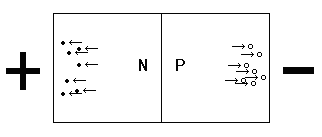
|
Reverse-biased P-N Junction
When the voltage applied to the N-Type side of the junction is more positive than that applied to the P-Type side, the junction is said to be reverse biased. The free electrons in the N-type silicon are pulled away from the junction by the positive voltage. The negative (less positive) voltage applied to the P-type appears to pull the holes away from the junction. This increases the size of the depletion region, assuring that the material will not conduct electricity. |
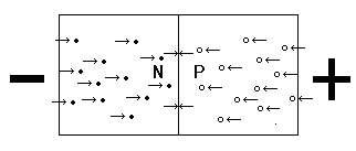
If you place a voltage across silicon with a P-N junction, with the N side more negative than the P side, you find that the holes in the P-type material are repelled by the more positive voltage and the donor electrons in the N-type material are repelled by the more-negative voltage. This causes the depletion region to become smaller as charge carriers are pushed toward the junction. If the voltage is strong enough, making the depletion region small enough, electrons from the N-type material will begin to cross the junction and fill the holes in the P-type material. When an electron fills a hole, both the electron and hole are no longer free to carry an electrical current. Essentially, the electron and hole each appear to cease to exist. When this happens, new electrons from the more-negative voltage and new holes from the more-positive voltage enter the crystal to replace the pairs that ceased to exist. At this point, the crystal is beginning to conduct electricity and the junction is said to be forward biased.
|
Forward-biased P-N Junction
When a positive potential is applied to the P-type side and a negative potential is applied to the N-type side, the junction is said to be forward biased. Free electrons are pushed toward the junction by the negative potential. Holes are pushed toward the junction by the positive potential. If enough voltage is applied, the electrons and holes are forced into the depletion region. With the crystal now filled with charge carriers it conducts electrical current. Holes and electrons meet at the junction and appear to cease to exist. These are replaced by the positive and negative potentials and current flows through the crystal. |
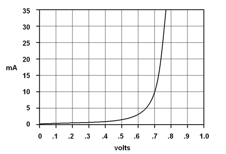
A forward-biased P-N junction will take a certain amount of voltage to force the current to start flowing. In the case of a silicon junction this takes approximately 0.5 volts. However, as the voltage is increased the current rises exponentially. As current rises, the voltage differential levels off just above 0.7 volts. Therefore, a forward-biased silicon P/N junction will typically have approximately 0.7 volts across it. A germanium P-N junction will begin to conduct at about 0.2 volts and will level off just above 0.3 volts. Therefore, a forward-biased germanium P/N junction will typically have 0.3 volts across it. Keep in mind that these voltages are typical for small devices at low currents. High power semiconductor devices can have several volts across their P-N junctions when conducting high currents.
|
A Typical Silicon P-N Junction, forward biased
At first, as the voltage across the junction increases the current increases very little; the junction looks like a relatively high resistance. As the voltage passes 0.5 volts, the current starts to increase more rapidly. After passing 0.7 volts, a tiny change in voltage causes a very large change in current. In this region the junction looks like a relatively low resistance. |
Myth:
A forward-biased silicon diode will always have 0.7 volts across it.
0.7 volts is a typical value. You can
almost bet that a
forward-biased silicon diode will have
somewhere around 0.7 volts across it. However, at high currents this
voltage can be significantly above 0.7 volts. For example,
according to the datasheet the common 1N4001 will have 1.0 volts across
it when conducting 1 amp of current. the 1N3670 will have 1.3 volts
across it when conducting 12 amps. Transistors can have even more.
Peak Inverse Voltage (PIV)
Normally, a P-N junction does not conduct when reverse biased. However, if enough voltage is applied, the junction will begin to conduct even when reverse biased. The voltage where this occurs is called the peak inverse voltage (PIV) and ranges from about 50 volts to several thousand volts, depending on the design of the device. If you exceed the PIV of most devices, the junction will break-down and the device will be damaged or destroyed.Majority and Minory Carriers
Semiconductor materials are not perfect. In P-type material there will be a few stray electrons. In N-type material there will be a few stray holes. N-type and P-type materials each contain both types of charge carriers, but in hugely different proportions. N-type material mostly has free electrons so electrons are called the majority carriers in N-type material. P-type material has mostly free holes so the holes are called the majority carriers in P-type material. In N-type material the stray holes are called minority carriers. Likewise, in P-type material the stray electrons are called the minority carriers.The main effect of minority carriers is called noise. This consists of tiny currents that are not part of the normal operation. For example, when a PN junction is reverse biased the minority carriers are on the wrong sides of the junction. The minority carriers actually form a forward-biased junction while the majority carriers form the reverse-biased junction. There are only a tiny number of minority carriers so the current across this junction is correspondingly tiny, but it does exist and sometimes has a significant effect on a circuit. On the other hand, minority carriers are manipulated to make transistors do what they do.
Semiconductors
| Vocademy |