| Vocademy |
Transistor Characteristics
| Note: this material is a bit advanced. You may want to skip it and come back later. You may want to come back later even if you don't skip it. Some of this material will also be covered again in Analog Circuits. |
Bi-polar Junction Transistors
The following circuit is an
example of a test circuit to demonstrate
the characteristics of a bi-polar junction transistor. Notice that
there are two current
paths, making this a parallel circuit. We have current flowing into the
base of the transistor (the base current, labeled IB) and
current flowing into the collector (the collector current, labeled IC).
These two currents exit the emitter together (the emitter current, IE,
not labeled in the diagram). According to Kirchhoff's Current Law
the current exiting the emitter must be the sum of the currents
entering the base and collector (see
Kirchhoff's Current Law). These
currents then split up again at
the bottom of the circuit where the emitter connects to the negative
terminals of the two batteries. The base current circulates in the left
part of the circuit (the base circuit) and the collector current
circulates in the right part of the circuit (the collector circuit).
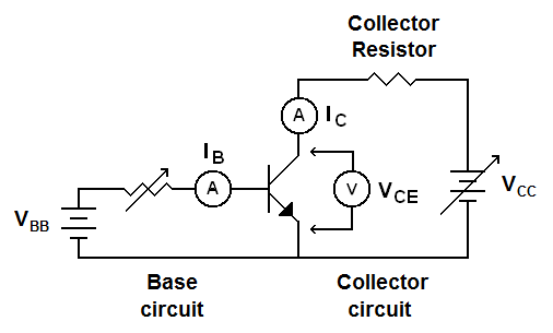
| Example test circuit for the following transistor curve. |
This is called a common-emitter
amplifier because the emitter of the transistor is common
to both circuits (the emitter connection is a common-connection type of
ground [see
What is Ground in
DC Circuits]).
We have two current meters to show that we are interested in the base
current and the
collector current. There is also a voltmeter showing that we are
interested in the voltage
between the collector and the emitter (the collector-to-emitter voltage
labeled VCE). The collector resistor isolates
the collector from the collector power supply (the battery labeled VCC).
Without this resistor the voltage at
the collector would always be the battery voltage. We need the
collector voltage to be able to drop as the collector current increases.[1]
The battery labeled VBB is there to supply current to the
base of the transistor. The variable resistor in the base circuit
controls the base
current.
Let's start by setting the base current to 20 μA. Holding the base current at 20 μA let's increase the battery voltage until VCE is 20 volts. The graph below shows what the the collector current (IC) does as we increase VCE.
Let's start by setting the base current to 20 μA. Holding the base current at 20 μA let's increase the battery voltage until VCE is 20 volts. The graph below shows what the the collector current (IC) does as we increase VCE.
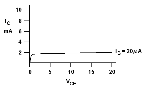
| Going from left to right VCE is increased. Notice that after an initial rise the collector current (IC) levels off and hardly changes as VCE increases. |
Notice that IC
levels off at about 2 mA and stays there regardless of VCE.
With this information we can calculate hFE, which is IC
divided by IB (see
Bi-polar Junction Transistors).
Here IC is 2 mA and IB
is 20
μA. Regardless of VCE,
IC is about 100 times IB so we have an hFE
of 100.
Now let's repeat the process with the base current set at 40 μA
Now let's repeat the process with the base current set at 40 μA
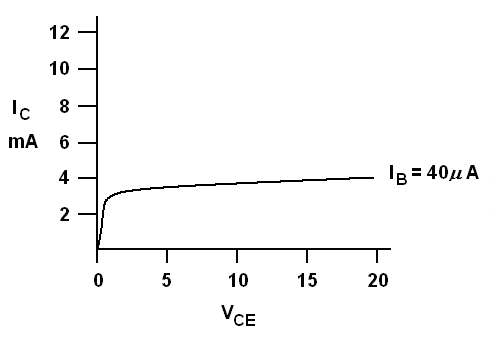
| The same transistor with a base current of 40 μA. Notice that the flat line isn't quite as flat. There is a slight increase in collector current as VCE is increased. |
Everything looks about the same
except the horizontal line is a bit
higher. This shows that doubling the base current just about doubled
the collector current. The collector current is now about 4 mA
regardless of VCE. Well, not really. Notice that the
horizontal line
isn't quite as horizontal. The slope was negligent with a base current
of 20
μA, but now it is quite
noticeable. At a VCE of 20 volts the collector current is
pretty close to 4 mA, but at a VCE of 5 volts IC
is closer to 3.5 mA.
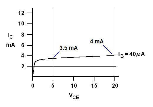
Does that mean that with a VCE of 20 volts hFE is 100 and with a VCE of 5 volts hFE is about 90? Yes, it does. It would be really nice if hFE were completely independent of all the other parameters, but it isn't. It's just something we have to deal with.
Now let's start over and draw graphs using base currents of 10 μA through 120 μA in 20 μA steps. When we are finished we have something like this:

| The collector current (IC) is lower at lower levels of VCE. |
Does that mean that with a VCE of 20 volts hFE is 100 and with a VCE of 5 volts hFE is about 90? Yes, it does. It would be really nice if hFE were completely independent of all the other parameters, but it isn't. It's just something we have to deal with.
Now let's start over and draw graphs using base currents of 10 μA through 120 μA in 20 μA steps. When we are finished we have something like this:
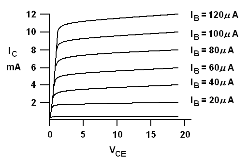
| A typical transistor curve (this curve is a close approximation of that for a 2N2222 transistor). |
In this graph each horizontal line
represents the collector current (IC) where the base (IB)
current is held at a different steady value (indicated to the right of
each line). As we increase the base current the horizontal line gets
higher, indicating a higher collector current. Going from left to right
the collector-to-emitter voltage (VCE) is increased. The
fact that each horizontal line is fairly flat shows that the collector
current is much more dependent on the current flowing into the base
than the voltage across the transistor.
When designing a transistor circuit we usually want to make sure the transistor operates under conditions where the collector current lines are fairly flat. In the above graph the slopes are reasonably flat throughout all the parameters. However, at higher base currents the slopes will get increasingly steep. You would want to avoid designing an amplifier that operates under those conditions. The output will be significantly distorted compared to the input.
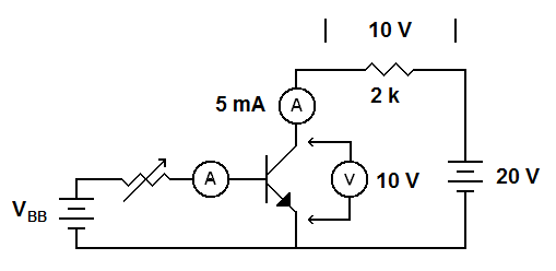
With a battery voltage (VCC) of 20 volts and a collector current of 5 mA we have 10 volts across the 2 k collector resistor. This leaves 10 volts for the collector-to-emitter voltage (VCE). That's 10 volts across the collector resistor and 10 volts for VCE. This adds up to the battery voltage and Kirchhoff's Voltage Law is satisfied (see Kirchhoff's Voltage Law).
Now let's increase the base current until the collector current is 7.5 mA.
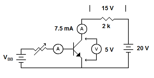
Now the voltage across the collector resistor has increased to 15 volts. There is a corresponding drop in VCE to 5 volts. Kirchhoff's Voltage Law is still satisfied.
Now lets increase the base current until the collector current is 10 mA.
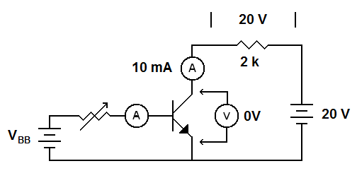
Now the voltage across the collector resistor is 20 volts. That's all the voltage the battery has to give. There is nothing left for VCE. It has to be 0 volts. Let's see what happens if we increase the base current further.
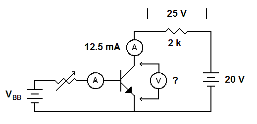
If we increase the base current until the collector current is 12.5 mA the voltage across the collector resistor will increase to 25 volts. But it can't. This violates Kirchhoff's Voltage Law. We cannot get more voltage than than the battery has to supply. With this 2 k resistor it is impossible to increase the collector current beyond 10 mA. We can still increase the base current, but regardless of what hFE says the collector current will not go above 10 mA. The circuit is saturated.
Actually, you cannot even get 20 volts across the collector resistor. The resistance of the transistor will try to go to 0 ohms when the transistor is saturated, but this is impossible. The collector-to-emitter path always has some resistance, so when there is current flowing into the collector there will be some voltage between the collector and the emitter. This is called the saturation voltage and is labeled VCE(sat) on transistor datasheets. The saturation voltage is typically around 0.4 volts but may be more for power transistors. For example, the 2N3055 has a saturation voltage of around 2 volts. Here is the above circuit with realistic saturation parameters.
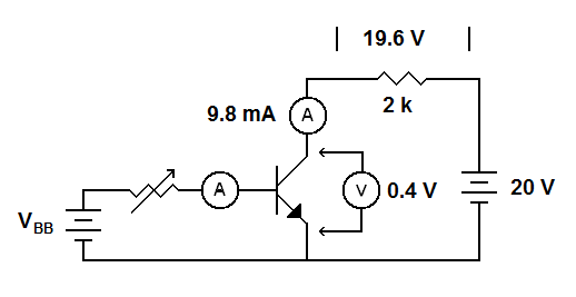
Now we have a VCE of 0.4 volts and the voltage across the collector resistor is 19.6 volts.
When designing a transistor circuit we usually want to make sure the transistor operates under conditions where the collector current lines are fairly flat. In the above graph the slopes are reasonably flat throughout all the parameters. However, at higher base currents the slopes will get increasingly steep. You would want to avoid designing an amplifier that operates under those conditions. The output will be significantly distorted compared to the input.
Saturation
As you increase the base current the collector current increases proportionally. However, you eventually reach a point where further increasing the base current no longer causes an increase in collector current. This condition is called saturation. The saturation point depends largely on the value of the collector resistor. Let's add some parameters to the above circuit and see what happens in both nominal operation and in saturation. We'll make the battery voltage 20 volts and increase the base current until the collector current is 5 mA. (We don't need to know the base current, We'll just turn the variable resistor until we see 5 mA for IC.)
|
Here is our
test circuit
in nominal operation. |
With a battery voltage (VCC) of 20 volts and a collector current of 5 mA we have 10 volts across the 2 k collector resistor. This leaves 10 volts for the collector-to-emitter voltage (VCE). That's 10 volts across the collector resistor and 10 volts for VCE. This adds up to the battery voltage and Kirchhoff's Voltage Law is satisfied (see Kirchhoff's Voltage Law).
Now let's increase the base current until the collector current is 7.5 mA.

|
The same circuit with the
collector current increased slightly. |
Now the voltage across the collector resistor has increased to 15 volts. There is a corresponding drop in VCE to 5 volts. Kirchhoff's Voltage Law is still satisfied.
|
Wait a
minute. The current through the transistor went up yet the
voltage across it went down. How can this be? In
DC Circuits we learned that as you
increase the current through a resistor the voltage across it
increases. Did
the resistance of the transistor go down as the current went up? It did. That's what transistors do. Remember that a BJT acts like a current-controlled variable resistor. Let's apply Ohm's law to the transistor and see what's going on. We have 5 volts across the transistor (VCE) and 7.5 milliamps flowing through it (IC). 5 volts divided by 7.5 milliamps gives us 666 ohms. 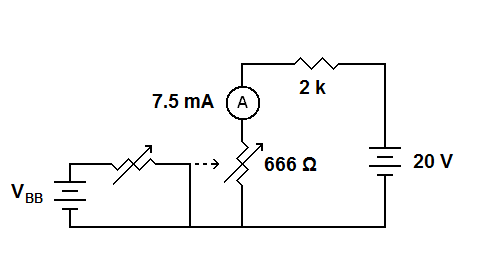
If we apply the rules for series circuits to the collector circuit we will see that it is acting like a 2k resistor and a 666 ohm resistor in series with a 20 volt battery. The transistor is acting like any 666 ohm resistor. All the rules we learned in DC circuits still apply. |
Now lets increase the base current until the collector current is 10 mA.

|
Now the collector current
has reached its limit with this collector resistor. |
Now the voltage across the collector resistor is 20 volts. That's all the voltage the battery has to give. There is nothing left for VCE. It has to be 0 volts. Let's see what happens if we increase the base current further.

|
Increasing the collector
current further causes a Kirchhoff's Voltage Law violation. |
If we increase the base current until the collector current is 12.5 mA the voltage across the collector resistor will increase to 25 volts. But it can't. This violates Kirchhoff's Voltage Law. We cannot get more voltage than than the battery has to supply. With this 2 k resistor it is impossible to increase the collector current beyond 10 mA. We can still increase the base current, but regardless of what hFE says the collector current will not go above 10 mA. The circuit is saturated.
Actually, you cannot even get 20 volts across the collector resistor. The resistance of the transistor will try to go to 0 ohms when the transistor is saturated, but this is impossible. The collector-to-emitter path always has some resistance, so when there is current flowing into the collector there will be some voltage between the collector and the emitter. This is called the saturation voltage and is labeled VCE(sat) on transistor datasheets. The saturation voltage is typically around 0.4 volts but may be more for power transistors. For example, the 2N3055 has a saturation voltage of around 2 volts. Here is the above circuit with realistic saturation parameters.

|
Here are realistic
parameters for a saturated transistor circuit.[2] |
Now we have a VCE of 0.4 volts and the voltage across the collector resistor is 19.6 volts.
|
Troubleshooting tip: If you have a
base-to-emitter voltage
that is significantly above 0.7 volts, don't automatically assume the
transistor is bad. Check the rest of the circuit
for voltages like those above. If it looks like that, the circuit is probably
saturated and the transistor is doing exactly what it is expected to
do. However, if you see signs of low collector current (like a VCE
equal to the battery voltage) you probably have a bad transistor or a
bad connection to the transistor.
Here's the chain of logic: If there is a high base-to-emitter voltage there must be a high base current. If there is a high base current there must be a high collector current. If there is a high collector current there must be a large voltage drop across the collector resistor. This results in a low VCE. That's what is happening above. However, if you have a high base current and VCE equals the battery voltage, this indicates that there is no collector current; there must be no current flowing through the collector resistor. The transistor must be bad, acting like an open circuit (see Open Circuits).[3] |
Cutoff
Just
as there is a point where increasing the base current no longer causes
an increase in collector current (saturation) there is a point where
decreasing the base current no longer causes a decrease in collector
current. This condition is called cutoff. Let's take another look at
that transistor curve.
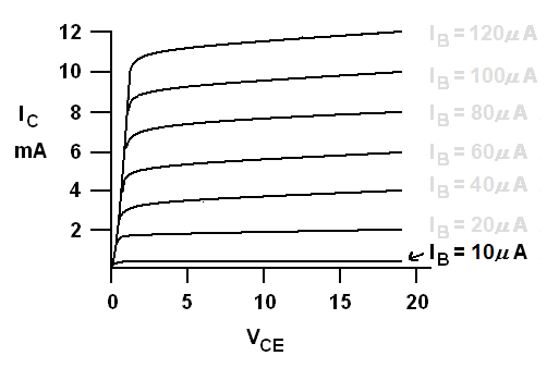
Take a look at the bottom collector current line. This is the line for a base current of 10 μA. This is the cutoff current. The cutoff current in this graph is a bit high for a real-world transistor, but every transistor has a collector current that is the lowest possible collector current regardless of how low the base current goes. This is called the collector cutoff current and is labeled ICEO (current from the collector to the emitter with the base open [no connection to the base]).

Take a look at the bottom collector current line. This is the line for a base current of 10 μA. This is the cutoff current. The cutoff current in this graph is a bit high for a real-world transistor, but every transistor has a collector current that is the lowest possible collector current regardless of how low the base current goes. This is called the collector cutoff current and is labeled ICEO (current from the collector to the emitter with the base open [no connection to the base]).
FETs
The following circuit is a common-soruce amplifier. It is the FET eqivalent of the common-emitter amplifier. We can use it to create a graph of and FET amplifier characteristics. The main difference is the labeling of the components and other parts of the circuit. Instead of a base current we have a gate-to-source voltage (VGS). Instead of a collector current we have a drain current (ID). The equivalent of VCE is VDS, etc.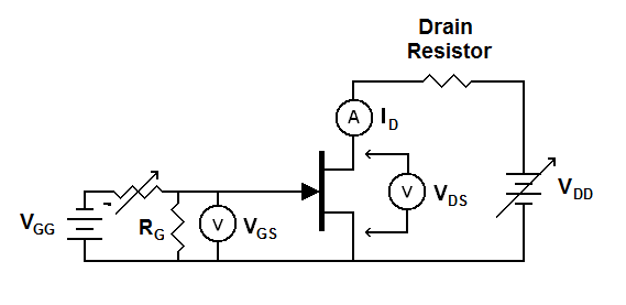
| FET version of the test circuit.[4] |
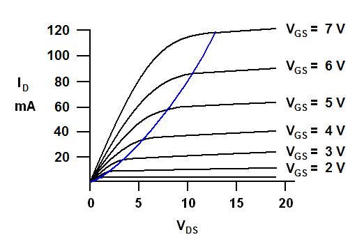
After after a procedure equivalent to the one used for a BJT we get a curve something like this.
|
FET Characteristic Curve |
There are several notable
differences between the BJT curver and the FET curve. The spacing of
the drain current
lines is not even; the relation of ID to VGS is
not as linear as the relationship of IC to IB.
There is a large area to the left of the diagram where the drain
current lines have notable curves. With this example, with a VDS
under 10 volts the drain current lines are far from flat. In this part
of the curve drain current
is significantly affected by VDS. These two parts of the
graph are divided by a blue line because they provide two different
ways to use an FET.
To the left of the blue line is the ohmic region. If operated in this region—with a VDS under 5 volts—the transistor has a resistance proportional to VGS rather than a drain current proportional to VGS. It acts like a voltage-controlled variable resistor. We have said all along that a transistor acts like variable resistor. However, in previous examples it acts like a variable resistor with some intelligence; the resistance changes to follow certain rules. In the ohmic region it acts more as if it simply changes its resistance in response to the gate voltage.
To the right of this the blue line is the saturation region[5]. In this region the FET operates much like a BJT, only it is voltage controlled instead of current controlled.
What is Saturation
| Vocademy |