| Vocademy |
FETs
There are two types of FETs. First we will look at Metal-Oxide-Semiconductor FETs (MOSFETs). These are true "field effect" transistors because electrostatic fields are used to attract or repel charge carries to control current flow. They are traditionally made of three layers of material: first a layer of aluminum (metal); then an insulating layer of silicon dioxide (oxide); and finally the main part of the transistor is made of silicon (semiconductor)—metal-oxide-semiconductor—MOS. Then we will look at Junction FETs (J-FETs). They control current flow by manipulating the size of the depletion region around a reverse-biased PN junction.MOSFETs
First let's look at an N-channel enhancement mode Metal-Oxide-Semiconductor Field Effect Transistor (a mouthful, isn't it). It is made from two areas of N-type silicon embedded in a block of P-type silicon (review Semiconductors).
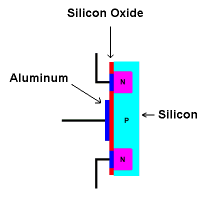 |
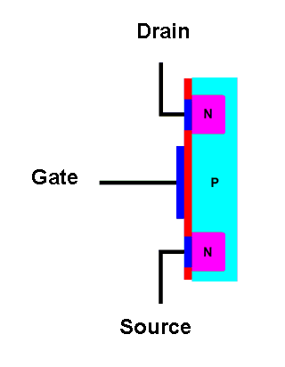 |
| An N-channel enhancement mode
MOSFET. |
The terminal connected to one N-type region is called the drain. This is where conventional current will enter the transistor. The terminal connected to the other N-type region is called the source. This is where where current will exit the transistor; conventional current goes into the drain and comes out of the source. A layer of metal (usually aluminum, blue in the diagram) is deposited onto the N-type regions to make electrical contact with them.
The gate terminal connects to a large area of metal that is deposited on a thin layer of insulating material (traditionally silicon oxide). There is no electrical connection between the gate and the conducting channel. MOS transistors are often called "insulated gate" transistors because of this feature. Now let's put a battery across the transistor and see what happens.
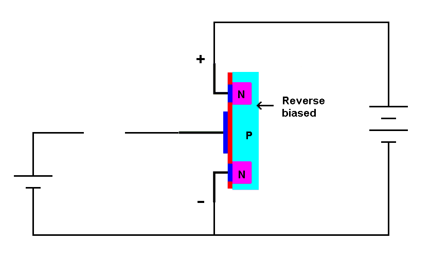
| When
connected to a battery in the proper configuration the PN junction
between the drain region and the P-type material is reverse biased. |
The positive terminal is connected to the drain and the negative terminal is connected to the source. There is no connection to the gate, but we have a battery there ready to connect when we need it. In this configuration the PN junction between the N-type drain region and the P-type body is reverse biased. Like any reverse-biased junction (such as a reverse-biased diode) no current can flow across this junction so current cannot flow between the drain and source.
Now let's take a look at the distribution of free electrons in the transistor.
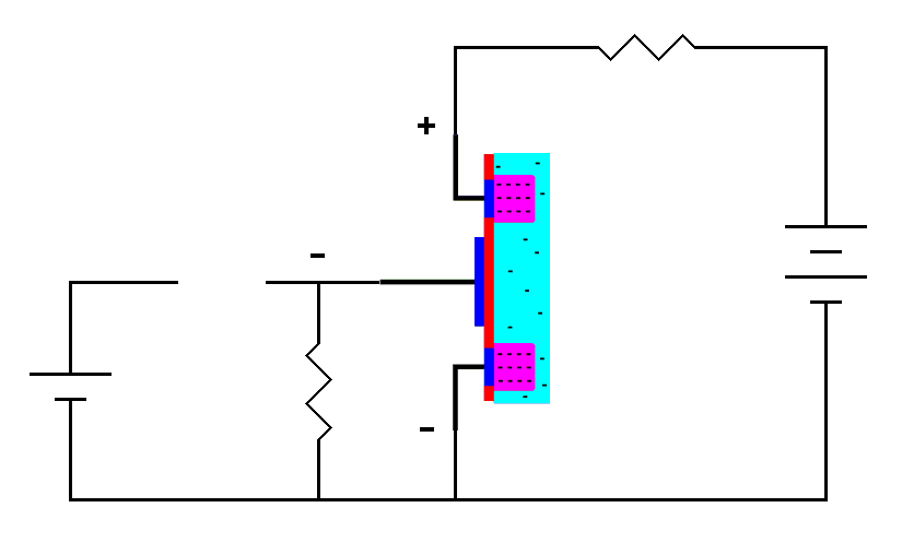
| The
P-type material has a few stray electrons (represented by minus
symbols). They don't do much now, but will come into play later. |
The N-type regions have an abundance of free electrons. Recall from Semiconductors that P-type material has a few stray free electrons called minority carriers. These stray electrons are scattered throughout the P-type material. Their effect is significant but tiny, so we will assume that they no effect at this point.
Now let's put some voltage on the gate of the transistor.
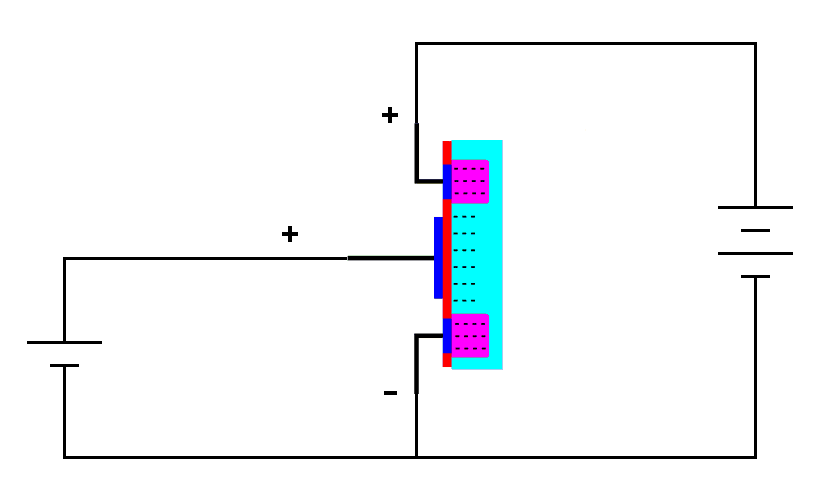
| When
a positive voltage is put on the gate stray electrons
are attracted to the gate region creating a conducting channel. |
The positive charge at the gate attracts the stray electrons into the gate region. This concentration of electrons overwhelms the characteristics of the P-type material making it act like N-type material. We now essentially have a region of N-type material extending from the drain to the source. There are no-longer any PN junctions, just a block of conductive N-type material. This creates a conductive channel and current will flow from the drain to the source through the transistor. This is called an enhancement mode MOSFET because the nonconductive channel is enhanced with electrons to make it conductive. It is called an N-channel MOSFET because free electrons in the conducting channel, although in P-type material, make it act like N-type material.
Complementary to the N-channel enhancement mode MOSFET there is a P-channel version. This works the same as the N-channel version except the voltages polarities are reversed. In normal operation the drain is connected to the negative terminal of the battery and the source is connected to the positive terminal. The gate is made negative to attract stray holes scattered around the N-type material into the conducting channel. Conventional current flows into the source and out of the drain.
Now let's look at an N-channel depletion mode MOSFET.
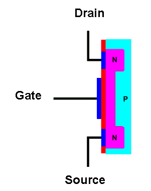
| The N-channel depletion mode
MOSFET has a small channel of N-type material between the drain and the
source. |
This is constructed like the N-channel enhancement mode MOSFET except there is a channel of N-type material between the drain and source. This channel is already conductive when there is no voltage on the gate.
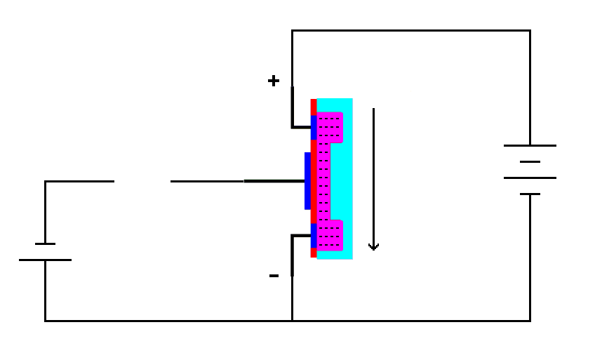
| When there is no voltage on the
gate the transistor conducts current through the N-type material in the
conductive channel. |
Now let's put a negative voltage on the gate and see what happens.
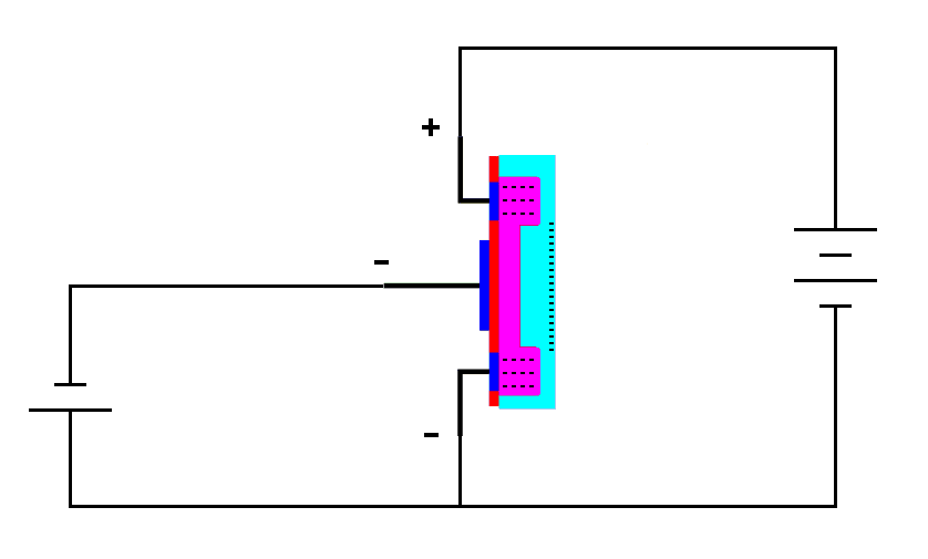
| A negative voltage on the gate
drives electrons out of the conducting channel. |
The negative voltage on the gate drives electrons out of the conducting channel. This stops the current flow through the transistor. This is opposite to an enhancement mode N-channel MOSFET. There, a positive voltage at the gate turns the transistor "on". Here, a negative voltage at the gate turns the transistor "off". There is also an P-channel version of the depletion mode MOSFET that works with opposite polarity.
An useful feature of depletion mode MOSFETs is that they can also act much like enhancement mode MOSFETs. Look at what happens if we put a positive voltage on the gate of the N-channel depletion mode MOSFET.
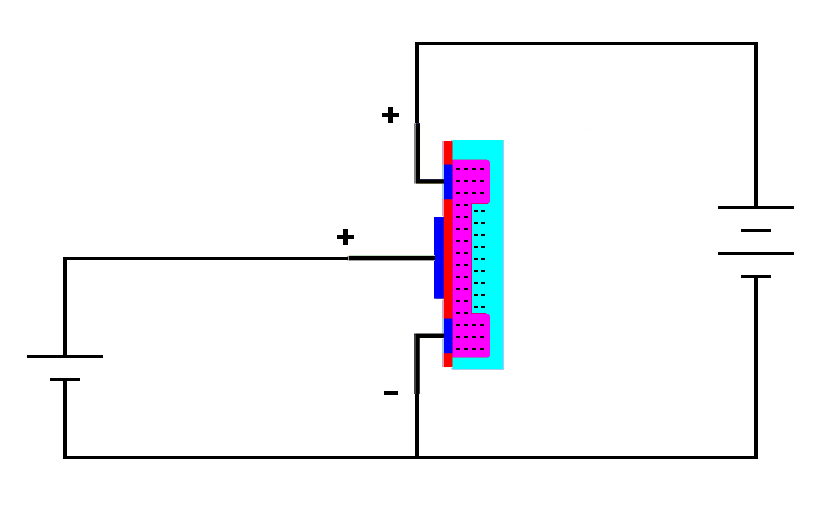
| A positive voltage on the gate
of an N-channel depletion mode MOSFET pulls more electrons into the
conducting channel. |
The positive charge on the gate pulls even more electrons into the conduction channel, making the depletion mode MOSFET act like an enhancement mode MOSFET.
Static Electricity Precautions
MOS transistors are very sensitive to static electricity. Even low voltages of static electricity can damage the insulation between the gate and the conductive channel. Modern MOS transistors have protection in the form of zener diodes between the gate and the other terminals.[1] Nevertheless, antistatic precautions should be taken when working with MOS devices.MOSFET Schematic Symbols
There are more schematic symbols for MOSFETs than there are types of MOSFETs. Let's take a look at them.Enhancement mode MOSFET symbols
| N-channel |
P-channel |
|
| Traditional |
 |
 |
| Simplified |
 |
 |
| Digital |
 |
 |
| Enhancement
mode MOSFET symbols. |
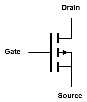
Enhancement mode MOSFET symbols have a solid line representing the gate and a dashed line representing the channel. The dashed line reminds us that the channel is nonconductive until a voltage is placed on the gate. The arrow indicates the orientation of the drain-to-gate PN junction. Like the zener diode, this junction is reverse biased in normal operation so the arrow points against conventional current flow. The arrow of an N-channel MOSFET points into the transistor, so remember that "N-channel points N". Sometimes the bulk or body connection, that's the connection with the arrow, connects to a separate fourth terminal on the MOSFET package. This is usually just tied to the source terminal. Any other use of this terminal is beyond the scope of this discussion.
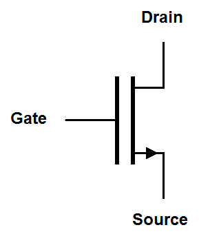
Many people don't think things are complicated enough so they have created additional "simplified" symbols for MOSFETs. The FET mode is indicated by the thickness of the line between the drain and the sorurce. The direction of The arrow indicates the orientation of the gate-to-source PN junction. It arrow points in the opposite direction to the traditional symbol. It also points in the direction of conventional current flow. I actually prefer the simplified symbols because they are similar to the symbols for bi-polar junction transistors.
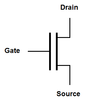
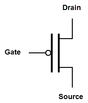
If this isn't confusing enough there are symbols without arrows popular with digital circuits. The channel type is indicated by the presence or absence of a circle on the gate. The absence of the circle indicates that the transistor is turned "on" by a positive voltage. The presence of the circle indicates that the transistor is turned "on" by a negative voltage.
Depletion Mode MOSFET Symbols
| N-channel |
P-channel |
|
| Traditional |
 |
 |
| Simplified |
 |
 |
| Digital |
 |
 |
| Depletion
mode MOSFET symbols. |
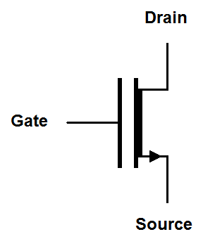
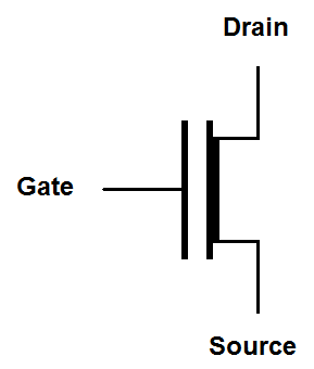
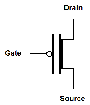
Depletion mode MOSFET symbols have a solid line representing the gate and a solid line representing the channel. The solid line for the channel reminds us that the channel is conductive until a voltage is placed on the gate. The simplified and digital symbols use a thick line to represent the existence of a conductive channel with no gate voltage.
Interchangeability of the Drain and Source with MOSFETs
You may have noticed that the drain and source regions look alike. Are
they interchangeable? The short answer is no. The actual construction
of the transistor has differences between the drain region and the
source region. Some MOSFETs have an internal diode between the drain
and source that is reverse biased in normal operation. If you try to
reverse the drain and source connections you will forward-bias this
diode, essentially creating a short circuit between the drain and
source. Also, as you can see in the traditional schematic symbol, the
body connection (the one with the arrow) is connected to the source
internally. This also complicates any potential interchangeability. Junction Field Effect Transistors
A junction Field Effect Transistor or J-FET is essentially a diode with two connections on one side of the junction. The following example is an N-channel J-FET.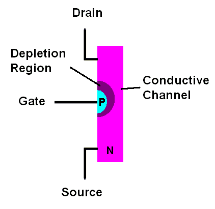
| An N-channel
J-FET |
With the N-channel J-FET the gate terminal is connected to P-type material and the drain and source terminals are connected to a single block of N-type material. Let's connect a battery across the drain and source and see what happens.
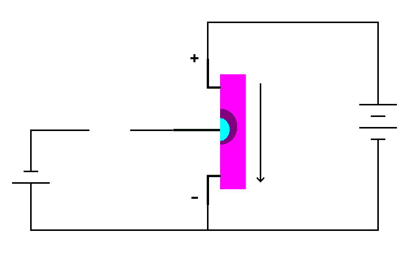
| An N-channel J-FET with no gate
voltage. |
The depletion region extends only part way into the N-type material. This leaves a contiguous block of N-type material where current will readily flow. With no voltage on the gate, current will flow from the drain to the source through the transistor. Now let's put some voltage on the gate.
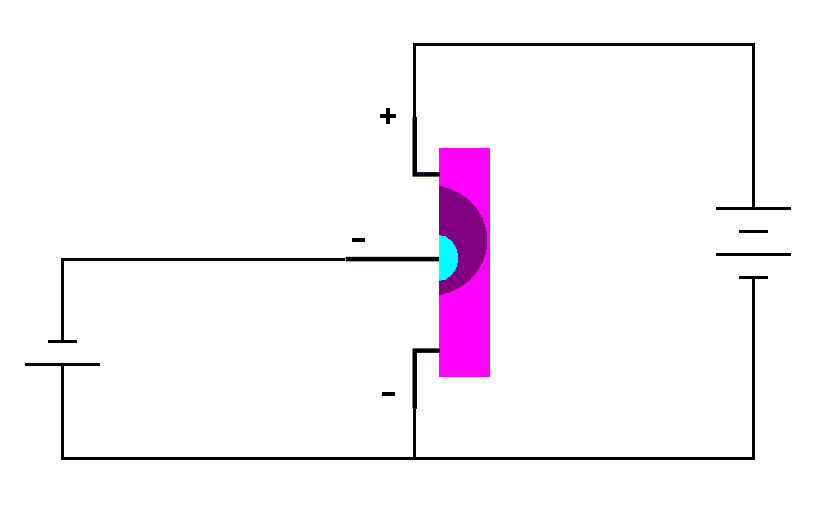
| With
a negative voltage applied to the gate the depletion region grows. If
the gate voltage is high enough the depletion can completely block
current flow. |
The gate voltage is now lower than the voltages at either the drain or the source. This reverse biases the PN junction making the depletion region larger (review Semiconductors) blocking the flow of current through the transistor (the depletion region is larger toward the drain because the voltage difference between the drain and the gate is greater than the voltage difference between the source and the gate). The gate voltage must be lower (more negative) than the source voltage. Otherwise the junction will become forward biased. Since the PN junction is reverse biased very little current flows through the gate. Therefore, very little current is required to operate a J-FET. The J-FET has a lower gate impedance than a MOSFET, but it still has a very high impedance.
A P-channel J-FET works the same as an N-channel J-FET except the voltage polarities are reversed.
J-FET symbols
| N-channel |
P-channel |
|||
| Drain |
Drain |
|||
| Gate |
 |
|
Gate |
 |
| Source |
Source |
|||
| Drain |
Drain |
|||
Gate |
 |
Gate |
 |
|
| Source |
Source |
| J-FET Symbols |
There are only two symbols for J-FETs. The N-channel symbol has the arrow on the gate terminal pointing inward and the P-channel has the arrow pointing outward. Sometimes the gate terminal is drawn in line with the source terminal. Some sources say that when the gate is in the center of the symbol it indicates an FET with drain and source terminals that can be swapped. However, you cannot rely on this. Always check the datasheet for device specifications.
Interchangeability of the Drain and Source with J-FETs
The drain and source terminals of a J-FET may be swappable. Refer to
the transistor datasheet for an individual transistor to see if they
can be swapped.MOSFETs
J-FETs
Transistorized
| Vocademy |