| Vocademy |
Bi-polar Junction Transistors (BJTs)
A bi-polar junction transistor is made of three layers of silicon in a
P-N-P or N-P-N arrangement.
| Collector |
|
Collector |
||
| Base |
 |
Base |
 |
|
| Emitter |
Emitter |
|||
| NPN |
PNP |
| Standard
model of a BJT. |
Each layer of silicon is connected to an
external lead. These connections are called the collector, the emitter
and the
base. The collector is analogous to the drain of an FET, the base is
analogous to the gate and the emitter is analogous to the source. With
an NPN transistor conventional current enters the collector and exits
the emitter.
A BJT acts like a current-controlled valve. With an NPN transistor, a small amount of conventional current injected into the base causes a large conventional current to flow from the collector to the emitter. The more current injected into the base, the more current flows from the collector to the emitter.
A BJT acts like a current-controlled valve. With an NPN transistor, a small amount of conventional current injected into the base causes a large conventional current to flow from the collector to the emitter. The more current injected into the base, the more current flows from the collector to the emitter.
The BJT as a Current-controlled Variable Resistor
The LGM model shown in the introduction is for an FET. Here is the LGM
model for a bi-polar junction transistor.
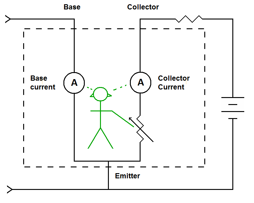
| The bi-polar junction transistor LGM model. The little green man watches the two current meters. His instructions are to make the variable resistor whatever resistance it takes to keep the collector current at some value related to the base current. |
In the bi-polar junction transistor LGM model there are two current
meters. One monitors
the base current and the other monitors the collector current. The
little green man controls a variable resistor that is between the
collector and the emitter. His job is to change the
variable resistor to whatever value it takes to keep the collector
current at some value related to the base current. For example, his
instructions may be to keep the collector current at 50 times the base
current (the input to output relationship is simpler with a BJT than an
FET).
A PNP transistor has opposite polarity compared to an NPN transistor and the current flows the opposite direction. With an NPN transistor conventional current flows into the base. This causes even more current to flow into the collector and out of the emitter. With a PNP transistor conventional current flows out of the base. This causes even more current to flow into the emitter and out of the collector (the names "collector" and "emitter" are clearly based on the NPN transistor).
A PNP transistor has opposite polarity compared to an NPN transistor and the current flows the opposite direction. With an NPN transistor conventional current flows into the base. This causes even more current to flow into the collector and out of the emitter. With a PNP transistor conventional current flows out of the base. This causes even more current to flow into the emitter and out of the collector (the names "collector" and "emitter" are clearly based on the NPN transistor).
| NPN Transistor |
|
 |
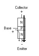 |
| A small current from the base to the emitter causes a large current from the collector to the emitter. |
| PNP Transistor | |
 |
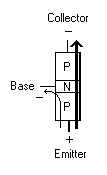 |
| A PNP transistor works like an NPN transistor except the voltage polarities are reversed. Note that the current flows in the opposite direction. |
BJT Schematic symbols
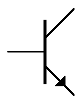
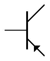
The following illustrations show the schematic symbols for bi-polar junction transistors.| NPN |
PNP |
|||
| Collector |
Collector | |||
| Base |
 |
|
Base |
 |
| Emitter | Emitter |
For the NPN transistor the arrow is on the emitter pointing outward, in
the direction of conventional current. For the PNP transistor the arrow
is also on the emitter, but pointing inward, also in the direction of
conventional current. To help remember which way the arrow points
some people say that with an NPN transistor the arrow is "Not Pointing
N" (not pointing in) where with a PNP transistor the arrow is "Pointing
N Positively" (pointing in positively).
Base-to-emitter voltage
Myth:
The base-to-emitter voltage (VBE)
of a
silicon bipolar junction transistor is always 0.7 volts.
As with diodes,
0.7 volts is a typical value. Also as with diodes you can
almost bet that under normal
operation a silicon BJT will have
somewhere around 0.7 volts between the base and the emitter. However,
just like any other forward-biased PN junction, this voltage
depends on the current flowing through the junction. For example,
according to the datasheet a 2N3055 will have a base-to-emitter voltage
(VBE)
of about 1.5 volts when it has a base current of around 115 mA (and
will have a collector current of about 4 amps). That's under normal
operation. When saturated (see
Transistor
Characteristics) the VBE has a maximum of 7
volts (that's 7 volts, not 0.7 volts) with a base current of 7 amps.
Even the low power 2N2222 may have a VBE of up to 6 volts
when heavily saturated. The
base current of a perfectly good transistor can be anywhere from 0
volts to several volts. Never automatically assume that a transistor is
bad just because the base-to-emitter voltage is something other than
0.7 volts.
The base-to-emitter voltage of a
germanium BJT is typically around
0.3 volts. However, this is subject to the same conditions as a silicon
transistor.
A reverse-biased base-to-emitter junction acts like a zener diode, with a typical operating voltage of around 5 volts. If you need a zener diode in a pinch you can use a BJT.
A reverse-biased base-to-emitter junction acts like a zener diode, with a typical operating voltage of around 5 volts. If you need a zener diode in a pinch you can use a BJT.
Lecture: Day 4 - Bipolar Junction Transistors
How a Transistor Works
Why do Junction Transistors Amplify Current and Not Voltage
Answers to Questions - Is a Transistor a Variable Resistor
| Vocademy |
